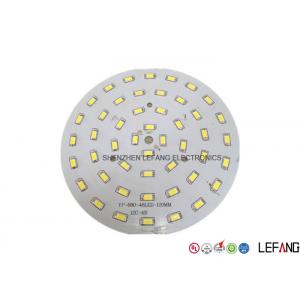
FR4 2 Layers LED PCB Board for Traffic and Street Lighting with LF - HASL
LED PCB Board could be used into numerous lighting application, such as traffic lighting, automotive headlights, street lighting, signal lighting, and so on. Particularly, alumimum is usually used to manufacture LED PCB Board for LED applications. That's because the alumimum PCB board could transfer and dissipate heat better than the traditional rigid printed circuit board.
Why choose LEFANG?
Established in 1999, Lefang owns 3 modern Printed Circuit Board factories in Guangdong, China.
We provide One-stop solution for PCB & PCBA manufacturing to our customers home and abroad.
High quality PCB products, competitive price, on time delivery, after-sale service are always offered.
To make the continued progress, we try our best to in every section, including selecting quality raw materials
strictly, imported advanced automated equipments, employing 70 experienced engineers, acquiring global
certification of ISO9001:2008, ISO14001:2004, ISO/TS16949:2009, UL, QC080000, OHSA18000, etc.
Our customers' industry come from Communication, Industrial Control, Automotive, Medical Equipment,
Security Apparatus, Consumer Electronics and LED Lighting.
We sincerely pursue win-win business with customer all the time!
How to get quick quotation?

| Step 1 Please send us Gerber file with these format: .CAD / .Gerber / .PCB / .DXP / .P-CAD, etc |
| Step 2 Also please provide us the below details for quick quotation: |
|
Board material: Fr - 4 / CEM - 1 / CEM - 3 / 22F / Fr - 1 / others
|
| Material brand: SY / KB / Rogers (optional) |
| Material Specification:High Tg / copper based / aluminum based or others (optional) |
| Board thickness: 0.1 - 6.0 mm |
| Copper thickness: 0.05 Oz - 8 Oz ( 17 um - 288 um ) |
| Surface Treatment: OSP / ENIG / HASL / Lead Free HASL / Immersion Tin / Immersion Sin |
| Color of solder mask and silk print: Green / red / blue / black / white / yellow ,etc |
| Board size and quantity |
|
If you don't have Gerber file, please provide us the imfomation as step 2 or post your PCB Board to us for clone.
|
|
SAMPLE:
|
|
Board Basic Info - SAMPLE
|
|
Board material
|
Fr - 4
|
|
Material brand
|
KB
|
|
Material Specification
|
Tg 170
|
|
Board thickness
|
1.6 mm
|
|
Copper thickness
|
1 Oz
|
|
Surface Treatment
|
ENIG
|
|
Solder mask / sSilk print
|
Green / White
|
|
Board size
|
100 mm * 100 mm
|
|
Quantity
|
10k
|
|
Lead Time
| Layer count |
Sample lead time/workday |
Batch lead time/workday |
| 1-2L |
2 |
6 |
| 4L |
5 |
8 |
| 6L |
5 |
9 |
| 8L |
6 |
10 |
| 10L |
8 |
10 |
| 12L |
8 |
12 |
| 14L |
10 |
15 |
| 16L |
10 |
18 |
| 18-40L (Up to difficulty) |
at least 18 |
at least 24 |
| P.S. For HDI, Blind/Buried Hole PCB: Regular Lead Time + 3 workdays |
How many advanced automated equipments do we have?
-- We have spent massively on purchasing below advanced automated production equipments.
| Equipment Name |
Plant in Shenzhen |
Plant in Dongguan |
| CCD exposure machine |
8 |
12 |
| AOI test machine |
6 |
8 |
| Mechanical drilling rig |
26 |
53 |
| Automatic edge finishing machine |
2 |
2 |
| Pressing machine |
2 |
2 |
| VCP |
0 |
2 |
| Electroplating line |
1 |
2 |
| CNC routing machine |
12 |
12 |
| Automatic tester |
10 |
16 |
Now send us your inquiry, and you will be replied within 8 hours!
Little knowledge - Double Sided PCB
Double Sided PCBs also known as Double-Sided Plated Thru or DSPT, which are the gateway to higher technology applications compared to single sided PCB.
Double Sided PCB allow for the routing of traces around each other by jumping between a top and bottom layer by way of vias.
The ability to cross paths from top to bottom greatly increasing the circuit designer's flexibility in circuits designing and lends itself to greatly increased circuit densities.