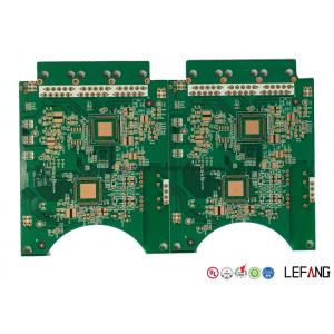
Multilayer 94V0 Fr4 Circuit Board PCB for Communication Electronics
This 94v0 fr4 PCB circuit board is made for communication electronics. we use Rogers FR - 4 raw material and Taiyo ink to guarantee quality of PCB board. The min.Line Trace Width/Space of this PCB board are
0.1 / 0.1 mm.

Why choose LEFANG?
Established in 1999, Lefang owns 3 modern Printed Circuit Board factories in Guangdong, China.
We provide One-stop solution for PCB & PCBA manufacturing to our customers home and abroad.
High quality PCB products, competitive price, on time delivery, after-sale service are always offered.
To make the continued progress, we try our best to in every section, including selecting quality raw materials
strictly, imported advanced automated equipments, employing 70 experienced engineers, acquiring global
certification of ISO9001:2008, ISO14001:2004, ISO/TS16949:2009, UL, QC080000, OHSA18000, etc.
Our customers' industry come from Communication, Industrial Control, Automotive, Medical Equipment,
Security Apparatus, Consumer Electronics and LED Lighting.
We sincerely pursue win-win business with customer all the time!
How to get quick quotation?
| Step 1 Please send us Gerber file with these format: .CAD / .Gerber / .PCB / .DXP / .P-CAD, etc |
| Step 2 Also please provide us the below details for quick quotation: |
|
Board material: Fr - 4 / CEM - 1 / CEM - 3 / 22F / Fr - 1 / others
|
| Material brand: SY / KB / Rogers (optional) |
| Material Specification:High Tg / copper based / aluminum based or others (optional) |
| Board thickness: 0.1 - 6.0 mm |
| Copper thickness: 0.05 Oz - 8 Oz ( 17 um - 288 um ) |
| Surface Treatment: OSP / ENIG / HASL / Lead Free HASL / Immersion Tin / Immersion Sin |
| Color of solder mask and silk print: Green / red / blue / black / white / yellow ,etc |
| Board size and quantity |
|
If you don't have Gerber file, please provide us the imfomation as step 2 or post your PCB Board to us for clone.
|
|
SAMPLE:
|
|
Board Basic Info - SAMPLE
|
|
Board material
|
Fr - 4
|
|
Material brand
|
KB
|
|
Material Specification
|
Tg 170
|
|
Board thickness
|
1.6 mm
|
|
Copper thickness
|
1 Oz
|
|
Surface Treatment
|
ENIG
|
|
Solder mask / sSilk print
|
Green / White
|
|
Board size
|
100 mm * 100 mm
|
|
Quantity
|
10k
|
|
Lead Time
| Layer count |
Sample lead time/workday |
Batch lead time/workday |
| 1-2L |
2 |
6 |
| 4L |
5 |
8 |
| 6L |
5 |
9 |
| 8L |
6 |
10 |
| 10L |
8 |
10 |
| 12L |
8 |
12 |
| 14L |
10 |
15 |
| 16L |
10 |
18 |
| 18-40L (Up to difficulty) |
at least 18 |
at least 24 |
| P.S. For HDI, Blind/Buried Hole PCB: Regular Lead Time + 3 workdays |
What kinds of test function will be offered?
| AOI (Automated Optical Inspection) |
Impedance control |
| Automatic short-circuit testing |
Metallographic microscope |
| RoHS detector |
Fly probe/ fixture mold |
| Dielectric tester |
Visual inspection |
Now send us your inquiry, and you will be replied within 8 hours!
Little knowledge - Medical Devices
Electronics contributes significantly to today's health-care industry like in diagnostic, monitoring and treatment devices. Because of the health implications associated with them, medical PCBs are held to higher standards than most other PCB types.
PCBs within the medical industry are highly specialized to satisfy the restriction of medical devices. In many medical applications, requirements like size and appearance are existed for an implant or emergency room monitor. For this reason, medical PCBs tend to be specialty high-density interconnect PCBs (HDI PCBs) or made with flexible base materials, allowing PCB to flex during use.