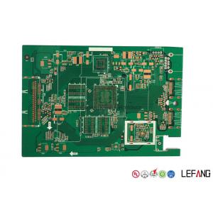
1.2mm 4 Layers OSP PCB Printed Circuit Board for Industrial Main Board
Mainboard used in different device have its demand. This pcb board is designed to used in industrial.
The board thickness 1.2 mm is thicker than normal 1.6mm in other pcb board. The surface treatment is OSP.

Why choose LEFANG?
-- Lefang provides One-Stop solution to save your cost and time.
| Quick Quotation - Competitive factory price is always offered |
| Free Sample - Sample for free before mass production |
| Quality Control - Sales Team monitors the production quality and lead time |
| On Time Delivery - Customize the logistics plan according to customer’s requirement |
|
After-sale Service - Reply to the claim within 24 hours to make sure our customer’s manufacturing
|
How to get quick quotation?
| Step 1 Please send us Gerber file with these format: .CAD / .Gerber / .PCB / .DXP / .P-CAD, etc |
| Step 2 Also please provide us the below details for quick quotation: |
|
Board material: Fr - 4 / CEM - 1 / CEM - 3 / 22F / Fr - 1 / others
|
| Material brand: SY / KB / Rogers (optional) |
| Material Specification:High Tg / copper based / aluminum based or others (optional) |
| Board thickness: 0.1 - 6.0 mm |
| Copper thickness: 0.05 Oz - 8 Oz ( 17 um - 288 um ) |
| Surface Treatment: OSP / ENIG / HASL / Lead Free HASL / Immersion Tin / Immersion Sin |
| Color of solder mask and silk print: Green / red / blue / black / white / yellow ,etc |
| Board size and quantity |
|
If you don't have Gerber file, please provide us the imfomation as step 2 or post your PCB Board to us for clone.
|
|
SAMPLE:
|
|
Board Basic Info - SAMPLE
|
|
Board material
|
Fr - 4
|
|
Material brand
|
KB
|
|
Material Specification
|
Tg 170
|
|
Board thickness
|
1.6 mm
|
|
Copper thickness
|
1 Oz
|
|
Surface Treatment
|
ENIG
|
|
Solder mask / sSilk print
|
Green / White
|
|
Board size
|
100 mm * 100 mm
|
|
Quantity
|
10k
|
|
Lead Time
| Layer count |
Sample lead time/workday |
Batch lead time/workday |
| 1-2L |
2 |
6 |
| 4L |
5 |
8 |
| 6L |
5 |
9 |
| 8L |
6 |
10 |
| 10L |
8 |
10 |
| 12L |
8 |
12 |
| 14L |
10 |
15 |
| 16L |
10 |
18 |
| 18-40L (Up to difficulty) |
at least 18 |
at least 24 |
| P.S. For HDI, Blind/Buried Hole PCB: Regular Lead Time + 3 workdays |
How many advanced automated equipments do we have?
-- We have spent massively on purchasing below advanced automated production equipments.
| Equipment Name |
Plant in Shenzhen |
Plant in Dongguan |
| CCD exposure machine |
8 |
12 |
| AOI test machine |
6 |
8 |
| Mechanical drilling rig |
26 |
53 |
| Automatic edge finishing machine |
2 |
2 |
| Pressing machine |
2 |
2 |
| VCP |
0 |
2 |
| Electroplating line |
1 |
2 |
| CNC routing machine |
12 |
12 |
| Automatic tester |
10 |
16 |
Now send us your inquiry, and you will be replied within 8 hours!
Little knowledge - Single Sided PCB
Single sided PCB contains only one layer of conductive material, where components are focused on one side, and the other side of the wire is concentrated.
Single sided PCB are the best choice for low density designs. They are easily designed and quickly manufactured to serve as the most cost effective platform in the industry.
For surface finishes, single sided boards are available for Organic surface protectant (OSP), Immersion Silver, Tin, and Gold plating along with both leaded or lead-free Hot Air Solder Level (HASL), with operating temperatures range from 130℃ to 230℃.