One-Stop Service Industrial PCB Board Printed Circuit for Control System
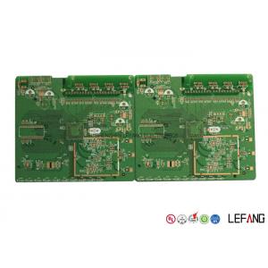
The multilayer PCB is design by our engineer. The layer count is 4 layers. This pcb board is used in industrial control systerm. Taconic high Tg fr4 material is used in this product. The board thickness is 111 * 100 mm. Copper thickness of the pcb board is 1 Oz / 35 µm.

Why choose LEFANG?
-- Lefang provides One-Stop solution to save your cost and time.
| Quick Quotation - Competitive factory price is always offered |
| Free Sample - Sample for free before mass production |
| Quality Control - Sales Team monitors the production quality and lead time |
| On Time Delivery - Customize the logistics plan according to customer’s requirement |
|
After-sale Service - Reply to the claim within 24 hours to make sure our customer’s manufacturing
|
How to get quick quotation?
| Step 1 Please send us Gerber file with these format: .CAD / .Gerber / .PCB / .DXP / .P-CAD, etc |
| Step 2 Also please provide us the below details for quick quotation: |
|
Board material: Fr - 4 / CEM - 1 / CEM - 3 / 22F / Fr - 1 / others
|
| Material brand: SY / KB / Rogers (optional) |
| Material Specification:High Tg / copper based / aluminum based or others (optional) |
| Board thickness: 0.1 - 6.0 mm |
| Copper thickness: 0.05 Oz - 8 Oz ( 17 um - 288 um ) |
| Surface Treatment: OSP / ENIG / HASL / Lead Free HASL / Immersion Tin / Immersion Sin |
| Color of solder mask and silk print: Green / red / blue / black / white / yellow ,etc |
| Board size and quantity |
|
If you don't have Gerber file, please provide us the imfomation as step 2 or post your PCB Board to us for clone.
|
|
SAMPLE:
|
|
Board Basic Info - SAMPLE
|
|
Board material
|
Fr - 4
|
|
Material brand
|
KB
|
|
Material Specification
|
Tg 170
|
|
Board thickness
|
1.6 mm
|
|
Copper thickness
|
1 Oz
|
|
Surface Treatment
|
ENIG
|
|
Solder mask / sSilk print
|
Green / White
|
|
Board size
|
100 mm * 100 mm
|
|
Quantity
|
10k
|
|
Lead Time
| Layer count |
Sample lead time/workday |
Batch lead time/workday |
| 1-2L |
2 |
6 |
| 4L |
5 |
8 |
| 6L |
5 |
9 |
| 8L |
6 |
10 |
| 10L |
8 |
10 |
| 12L |
8 |
12 |
| 14L |
10 |
15 |
| 16L |
10 |
18 |
| 18-40L (Up to difficulty) |
at least 18 |
at least 24 |
| P.S. For HDI, Blind/Buried Hole PCB: Regular Lead Time + 3 workdays |
How many advanced automated equipments do we have?
-- We have spent massively on purchasing below advanced automated production equipments.
| Equipment Name |
Plant in Shenzhen |
Plant in Dongguan |
| CCD exposure machine |
8 |
12 |
| AOI test machine |
6 |
8 |
| Mechanical drilling rig |
26 |
53 |
| Automatic edge finishing machine |
2 |
2 |
| Pressing machine |
2 |
2 |
| VCP |
0 |
2 |
| Electroplating line |
1 |
2 |
| CNC routing machine |
12 |
12 |
| Automatic tester |
10 |
16 |
Now send us your inquiry, and you will be replied within 8 hours!
Little knowledge - PCB Circuit Board
A printed circuit board (PCB) mechanically supports and electrically connects electronic components using conductive tracks, pads and other features etched from copper sheets laminated onto a non-conductive substrate.
Components (e.g. capacitors, resistors or active devices) are generally soldered on the PCB. Advanced PCBs may contain components embedded in the substrate.
There are three kinds of PCB, including single sided pcb (one copper layer), double sided pcb (two copper layers)and multi-layer pcb (outer and inner layers).
Conductors on different layers are connected with vias. Multilayer PCBs allow for much higher component density.