Multilayer High Frequency PCB board for Medical Photometer Devices Printed Circuit Board Taconic
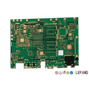
The 6 layers high frequency PCB Board is made with FR4 Board material with 1 Oz / 35 µm copper thickness. Also, the board size of this high frequency PCB Board is 106 * 78 mm, with green solder mask and OSP surface treatment.

Why choose LEFANG?
-- Lefang provides One-Stop solution to save your cost and time.
| Quick Quotation - Competitive factory price is always offered |
| Free Sample - Sample for free before mass production |
| Quality Control - Sales Team monitors the production quality and lead time |
| On Time Delivery - Customize the logistics plan according to customer’s requirement |
|
After-sale Service - Reply to the claim within 24 hours to make sure our customer’s manufacturing
|
How to get quick quotation?
| Step 1 Please send us Gerber file with these format: .CAD / .Gerber / .PCB / .DXP / .P-CAD, etc |
| Step 2 Also please provide us the below details for quick quotation: |
|
Board material: Fr - 4 / CEM - 1 / CEM - 3 / 22F / Fr - 1 / others
|
| Material brand: SY / KB / Rogers (optional) |
| Material Specification:High Tg / copper based / aluminum based or others (optional) |
| Board thickness: 0.1 - 6.0 mm |
| Copper thickness: 0.05 Oz - 8 Oz ( 17 um - 288 um ) |
| Surface Treatment: OSP / ENIG / HASL / Lead Free HASL / Immersion Tin / Immersion Sin |
| Color of solder mask and silk print: Green / red / blue / black / white / yellow ,etc |
| Board size and quantity |
|
If you don't have Gerber file, please provide us the imfomation as step 2 or post your PCB Board to us for clone.
|
|
SAMPLE:
|
|
Board Basic Info - SAMPLE
|
|
Board material
|
Fr - 4
|
|
Material brand
|
KB
|
|
Material Specification
|
Tg 170
|
|
Board thickness
|
1.6 mm
|
|
Copper thickness
|
1 Oz
|
|
Surface Treatment
|
ENIG
|
|
Solder mask / sSilk print
|
Green / White
|
|
Board size
|
100 mm * 100 mm
|
|
Quantity
|
10k
|
|
Lead Time
| Layer count |
Sample lead time/workday |
Batch lead time/workday |
| 1-2L |
2 |
6 |
| 4L |
5 |
8 |
| 6L |
5 |
9 |
| 8L |
6 |
10 |
| 10L |
8 |
10 |
| 12L |
8 |
12 |
| 14L |
10 |
15 |
| 16L |
10 |
18 |
| 18-40L (Up to difficulty) |
at least 18 |
at least 24 |
| P.S. For HDI, Blind/Buried Hole PCB: Regular Lead Time + 3 workdays |
How to guarantee our high quality products?
-- We employ 70 professional engineers to ensure our high quality products.
| Department |
Headcount |
| Electronic Eng. |
13 |
| R&D Eng. |
15 |
| PE Eng. |
10 |
| CAM Eng. |
26 |
| MI Eng. |
6 |
Now send us your inquiry, and you will be replied within 8 hours!
Little knowledge - Thick copper PCB
Electronics are used in demanding environments and operate at higher currents in these days.
Thick copper PCB can help conduct heat away from components and withstand high current, satisfying the market of power conversion module boards which is used in automobile electronics and electric equipment.
Heavy copper PCBs means copper conductors 5 oz/ft2 – 19 oz/ft2 in inner and/or outer layers; sometimes defined as more than 4 oz per square foot (ft2).
These boards can be manufactured in a smaller footprint as they can contain multiple weights of copper on the same circuit layers.