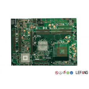
NVR Network Video Recorder Equipment Printed Circuit Board High Frequency PCB board For Security Monitor Taconic
The high frequency PCB is applied for security monitor devices, which is a 4 layers printed circuit board with 1.6 mm board thickness. Nowadays, high frequency PCB is used in wide range of area because it could provide faster signal flow rates to electronic components.

Why choose LEFANG?
-- Lefang provides One-Stop solution to save your cost and time.
| Quick Quotation - Competitive factory price is always offered |
| Free Sample - Sample for free before mass production |
| Quality Control - Sales Team monitors the production quality and lead time |
| On Time Delivery - Customize the logistics plan according to customer’s requirement |
|
After-sale Service - Reply to the claim within 24 hours to make sure our customer’s manufacturing
|
How to get quick quotation?
| Step 1 Please send us Gerber file with these format: .CAD / .Gerber / .PCB / .DXP / .P-CAD, etc |
| Step 2 Also please provide us the below details for quick quotation: |
|
Board material: Fr - 4 / CEM - 1 / CEM - 3 / 22F / Fr - 1 / others
|
| Material brand: SY / KB / Rogers (optional) |
| Material Specification:High Tg / copper based / aluminum based or others (optional) |
| Board thickness: 0.1 - 6.0 mm |
| Copper thickness: 0.05 Oz - 8 Oz ( 17 um - 288 um ) |
| Surface Treatment: OSP / ENIG / HASL / Lead Free HASL / Immersion Tin / Immersion Sin |
| Color of solder mask and silk print: Green / red / blue / black / white / yellow ,etc |
| Board size and quantity |
|
If you don't have Gerber file, please provide us the imfomation as step 2 or post your PCB Board to us for clone.
|
|
SAMPLE:
|
|
Board Basic Info - SAMPLE
|
|
Board material
|
Fr - 4
|
|
Material brand
|
KB
|
|
Material Specification
|
Tg 170
|
|
Board thickness
|
1.6 mm
|
|
Copper thickness
|
1 Oz
|
|
Surface Treatment
|
ENIG
|
|
Solder mask / sSilk print
|
Green / White
|
|
Board size
|
100 mm * 100 mm
|
|
Quantity
|
10k
|
|
Lead Time
| Layer count |
Sample lead time/workday |
Batch lead time/workday |
| 1-2L |
2 |
6 |
| 4L |
5 |
8 |
| 6L |
5 |
9 |
| 8L |
6 |
10 |
| 10L |
8 |
10 |
| 12L |
8 |
12 |
| 14L |
10 |
15 |
| 16L |
10 |
18 |
| 18-40L (Up to difficulty) |
at least 18 |
at least 24 |
| P.S. For HDI, Blind/Buried Hole PCB: Regular Lead Time + 3 workdays |
How to guarantee our high quality products?
-- We employ 70 professional engineers to ensure our high quality products.
| Department |
Headcount |
| Electronic Eng. |
13 |
| R&D Eng. |
15 |
| PE Eng. |
10 |
| CAM Eng. |
26 |
| MI Eng. |
6 |
Now send us your inquiry, and you will be replied within 8 hours!
Little knowledge - High frequency PCB
The increasing complexity and rapid change of electronic components require faster signal flow rates, and thus higher transmission frequencies.
A high-frequency PCB can meet your needs when incorporating a special signal requirement into your multilayer PCBs.
It offers a frequency range of 500MHz - 2GHz, making it ideally suited for high-speed designs, as well as radio frequency (RF), microwave and mobile applications.
High frequency PCB can also provide faster signal flow rates which is of great necessity in increasingly complex electronics.