Yello Ink Turnkey PCBA PCB Board Assembly for Consumer Electronics
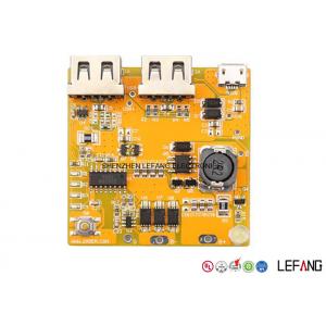
The surface treatment of the pcb board used is Immersion Silver, and the board and copper thickness are 1.6mm and 1 Oz which is normal in pcb. But the solder mask yellow is not very normal to find in pcb. it is a double sided pcb board.
Why choose LEFANG?
-- Lefang provides One-Stop solution to save your cost and time.
| Quick Quotation - Competitive factory price is always offered |
| Free Sample - Sample for free before mass production |
| Quality Control - Sales Team monitors the production quality and lead time |
| On Time Delivery - Customize the logistics plan according to customer’s requirement |
|
After-sale Service - Reply to the claim within 24 hours to make sure our customer’s manufacturing
|
How to get quick quotation?

| Step 1 Please send us Gerber file with these format: .CAD / .Gerber / .PCB / .DXP / .P-CAD, etc |
| Step 2 Also please provide us the below details for quick quotation: |
|
Board material: Fr - 4 / CEM - 1 / CEM - 3 / 22F / Fr - 1 / others
|
| Material brand: SY / KB / Rogers (optional) |
| Material Specification:High Tg / copper based / aluminum based or others (optional) |
| Board thickness: 0.1 - 6.0 mm |
| Copper thickness: 0.05 Oz - 8 Oz ( 17 um - 288 um ) |
| Surface Treatment: OSP / ENIG / HASL / Lead Free HASL / Immersion Tin / Immersion Sin |
| Color of solder mask and silk print: Green / red / blue / black / white / yellow ,etc |
| Board size and quantity |
|
If you don't have Gerber file, please provide us the imfomation as step 2 or post your PCB Board to us for clone.
|
|
SAMPLE:
|
|
Board Basic Info - SAMPLE
|
|
Board material
|
Fr - 4
|
|
Material brand
|
KB
|
|
Material Specification
|
Tg 170
|
|
Board thickness
|
1.6 mm
|
|
Copper thickness
|
1 Oz
|
|
Surface Treatment
|
ENIG
|
|
Solder mask / sSilk print
|
Green / White
|
|
Board size
|
100 mm * 100 mm
|
|
Quantity
|
10k
|
|
Lead Time
| Layer count |
Sample lead time/workday |
Batch lead time/workday |
| 1-2L |
2 |
6 |
| 4L |
5 |
8 |
| 6L |
5 |
9 |
| 8L |
6 |
10 |
| 10L |
8 |
10 |
| 12L |
8 |
12 |
| 14L |
10 |
15 |
| 16L |
10 |
18 |
| 18-40L (Up to difficulty) |
at least 18 |
at least 24 |
| P.S. For HDI, Blind/Buried Hole PCB: Regular Lead Time + 3 workdays |
How many advanced automated equipments do we have?
-- We have spent massively on purchasing below advanced automated production equipments.
| Equipment Name |
Plant in Shenzhen |
Plant in Dongguan |
| CCD exposure machine |
8 |
12 |
| AOI test machine |
6 |
8 |
| Mechanical drilling rig |
26 |
53 |
| Automatic edge finishing machine |
2 |
2 |
| Pressing machine |
2 |
2 |
| VCP |
0 |
2 |
| Electroplating line |
1 |
2 |
| CNC routing machine |
12 |
12 |
| Automatic tester |
10 |
16 |
Now send us your inquiry, and you will be replied within 8 hours!
Little knowledge - Medical Devices
Electronics contributes significantly to today's health-care industry like in diagnostic, monitoring and treatment devices. Because of the health implications associated with them, medical PCBs are held to higher standards than most other PCB types.
PCBs within the medical industry are highly specialized to satisfy the restriction of medical devices. In many medical applications, requirements like size and appearance are existed for an implant or emergency room monitor. For this reason, medical PCBs tend to be specialty high-density interconnect PCBs (HDI PCBs) or made with flexible base materials, allowing PCB to flex during use.