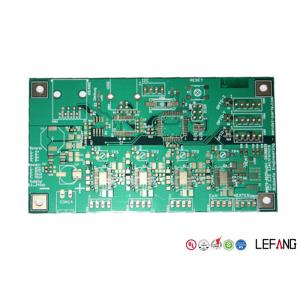
Double Sided PCB prototype for Automotive Electronics with UL Approval
The Double Sided PCB prototype is applied for Automotive Electronics with UL Approval, with 1.6 mm board thickness. This PCB prototype with ENIG surface treatment. The minimum aperture is 0.2 mm and green solder mask.
Why choose LEFANG?
Established in 1999, Lefang owns 3 modern Printed Circuit Board factories in Guangdong, China.
We provide One-stop solution for PCB & PCBA manufacturing to our customers home and abroad.
High quality PCB products, competitive price, on time delivery, after-sale service are always offered.
To make the continued progress, we try our best to in every section, including selecting quality raw materials
strictly, imported advanced automated equipments, employing 70 experienced engineers, acquiring global
certification of ISO9001:2008, ISO14001:2004, ISO/TS16949:2009, UL, QC080000, OHSA18000, etc.
Our customers' industry come from Communication, Industrial Control, Automotive, Medical Equipment,
Security Apparatus, Consumer Electronics and LED Lighting.
We sincerely pursue win-win business with customer all the time!
How to get quick quotation?

| Step 1 Please send us Gerber file with these format: .CAD / .Gerber / .PCB / .DXP / .P-CAD, etc |
| Step 2 Also please provide us the below details for quick quotation: |
|
Board material: Fr - 4 / CEM - 1 / CEM - 3 / 22F / Fr - 1 / others
|
| Material brand: SY / KB / Rogers (optional) |
| Material Specification:High Tg / copper based / aluminum based or others (optional) |
| Board thickness: 0.1 - 6.0 mm |
| Copper thickness: 0.05 Oz - 8 Oz ( 17 um - 288 um ) |
| Surface Treatment: OSP / ENIG / HASL / Lead Free HASL / Immersion Tin / Immersion Sin |
| Color of solder mask and silk print: Green / red / blue / black / white / yellow ,etc |
| Board size and quantity |
|
If you don't have Gerber file, please provide us the imfomation as step 2 or post your PCB Board to us for clone.
|
|
SAMPLE:
|
|
Board Basic Info - SAMPLE
|
|
Board material
|
Fr - 4
|
|
Material brand
|
KB
|
|
Material Specification
|
Tg 170
|
|
Board thickness
|
1.6 mm
|
|
Copper thickness
|
1 Oz
|
|
Surface Treatment
|
ENIG
|
|
Solder mask / sSilk print
|
Green / White
|
|
Board size
|
100 mm * 100 mm
|
|
Quantity
|
10k
|
|
How many advanced automated equipments do we have?
-- We have spent massively on purchasing below advanced automated production equipments.
| Equipment Name |
Plant in Shenzhen |
Plant in Dongguan |
| CCD exposure machine |
8 |
12 |
| AOI test machine |
6 |
8 |
| Mechanical drilling rig |
26 |
53 |
| Automatic edge finishing machine |
2 |
2 |
| Pressing machine |
2 |
2 |
| VCP |
0 |
2 |
| Electroplating line |
1 |
2 |
| CNC routing machine |
12 |
12 |
| Automatic tester |
10 |
16
|
Now send us your inquiry, and you will be replied within 8 hours!
How to reduce PCB cost
1. Improve the utilization ratio of the PCB substrate material. It is better to over 85 percents;
2. To make a bigger hole size of PCBs, which is no less than 0.3mm if possible and reduce the total amount of drilling holes;
3. The minimum trace width and space of PCBs is better no less than 4 mil, or the scrap rate will be increased 3 to 5 percents;
4. Reduce the board thickness of the printed circuit boards;
5. Enhance the universality of the main products.