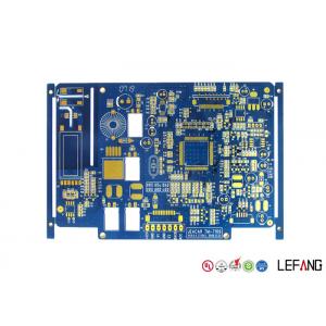
4Layers Immersion Gold PCB Board for Medical X-Ray Machine
The layer count of the copper base PCB Board is 4 layers, with 1.6 mm board thickness. The board line width and space are both 0.076 mm, with blue solder mask and ENIG surface treatment.
Why choose LEFANG?
Established in 1999, Lefang owns 3 modern Printed Circuit Board factories in Guangdong, China.
We provide One-stop solution for PCB & PCBA manufacturing to our customers home and abroad.
High quality PCB products, competitive price, on time delivery, after-sale service are always offered.
To make the continued progress, we try our best to in every section, including selecting quality raw materials
strictly, imported advanced automated equipments, employing 70 experienced engineers, acquiring global
certification of ISO9001:2008, ISO14001:2004, ISO/TS16949:2009, UL, QC080000, OHSA18000, etc.
Our customers' industry come from Communication, Industrial Control, Automotive, Medical Equipment,
Security Apparatus, Consumer Electronics and LED Lighting.
We sincerely pursue win-win business with customer all the time!
How to get quick quotation?

| Step 1 Please send us Gerber file with these format: .CAD / .Gerber / .PCB / .DXP / .P-CAD, etc |
| Step 2 Also please provide us the below details for quick quotation: |
Board material: Fr - 4 / CEM - 1 / CEM - 3 / 22F / Fr - 1 / others |
| Material brand: SY / KB / Rogers (optional) |
| Material Specification:High Tg / copper based / aluminum based or others (optional) |
| Board thickness: 0.1 - 6.0 mm |
| Copper thickness: 0.05 Oz - 8 Oz ( 17 um - 288 um ) |
| Surface Treatment: OSP / ENIG / HASL / Lead Free HASL / Immersion Tin / Immersion Sin |
| Color of solder mask and silk print: Green / red / blue / black / white / yellow ,etc |
| Board size and quantity |
If you don't have Gerber file, please provide us the imfomation as step 2 or post your PCB Board to us for clone.
|
SAMPLE:
|
Board Basic Info - SAMPLE | Board material | Fr - 4 | Material brand | KB | Material Specification | Tg 170 | Board thickness | 1.6 mm | Copper thickness | 1 Oz | Surface Treatment | ENIG | Solder mask / sSilk print | Green / White | Board size | 100 mm * 100 mm | Quantity | 10k |
|
How to guarantee our high quality products?
-- We employ 70 professional engineers to ensure our high quality products.
| Department | Headcount |
| Electronic Eng. | 13 |
| R&D Eng. | 15 |
| PE Eng. | 10 |
| CAM Eng. | 26 |
| MI Eng. | 6 |
Now send us your inquiry, and you will be replied within 8 hours!
How to improve the use ratio of PCB Board
1. Enlarge the PCB panel size, the larger panel, the less margin wasted;
2. Increase the pieces of PCB Board in each Sheet, which could also decrease the margin waste;
3. If two types of PCB such as A(big) and B(small), they could not reach a good use ratio when arrayed separately, then you could consider whether is suitable to array A and B in one sheet;
4. It is great to use professional software to arrange the PCB Board array.