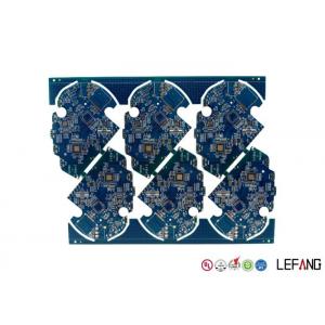
Customized Circuit Board PCB for Bluetooth Earphone
The 1 mm board thickness 4 layers PCB Board is applied to bluetooth earphone. While the surface treatment of the PCB Board is ENIG with blue solder mask. Also, the line width and spcaing of this PCB Circuit Board are both 0.1 mm, and the minimum aperture is 0.25 mm.
Technical Data
| Item | Details |
| Max layer count | 20 L |
| Max board thickness | 6.0 mm |
| Max aspect ratio | 10 : 1 |
| Max copper thickness | 6 OZ |
| Max dimension | 600 * 700mm |
| Min thickness of 4 layers PCB | 0.4 mm |
| Min hole / pad | 0.15 / 0.35mm |
| Hole location accuracy | + / - 0.05mm |
| PTH hole tolerance | + / - 0.05mm |
| Min line width and line space | 0.065 / 0.065mm |
| Surface treatment |
HASL / HASL lead free, OSP
Immersion gold/silver/tin, gold plating (hard gold and soft gold),
silver plating, tin plating, platinum plating, carbon ink,
ENEPIG
(electroless nickel - electroless palladium - immersion gold) |
How to get quick quotation?

| Step 1 Please send us Gerber file with these format: .CAD / .Gerber / .PCB / .DXP / .P-CAD, etc |
| Step 2 Also please provide us the below details for quick quotation: |
Board material: Fr - 4 / CEM - 1 / CEM - 3 / 22F / Fr - 1 / others |
| Material brand: SY / KB / Rogers (optional) |
| Material Specification:High Tg / copper based / aluminum based or others (optional) |
| Board thickness: 0.1 - 6.0 mm |
| Copper thickness: 0.05 Oz - 8 Oz ( 17 um - 288 um ) |
| Surface Treatment: OSP / ENIG / HASL / Lead Free HASL / Immersion Tin / Immersion Sin |
| Color of solder mask and silk print: Green / red / blue / black / white / yellow ,etc |
| Board size and quantity |
If you don't have Gerber file, please provide us the imfomation as step 2 or post your PCB Board to us for clone.
|
SAMPLE:
|
Board Basic Info - SAMPLE | Board material | Fr - 4 | Material brand | KB | Material Specification | Tg 170 | Board thickness | 1.6 mm | Copper thickness | 1 Oz | Surface Treatment | ENIG | Solder mask / sSilk print | Green / White | Board size | 100 mm * 100 mm | Quantity | 10k |
|
What kinds of quality Raw Materials will be used?
| Board Brand | ITEQ, SY, Isola. Rogers, Arlon, Nelco, Taconic, Hitachi, KB,etc |
| Potion | Rohm & Haas, Atotech, Umicore |
| Printing Ink | Taiyo, Rongda |
| Dry Film | Asahi, Dupont, Etertec
|
Now send us your inquiry, and you will be replied within 8 hours!
How to improve the use ratio of PCB Board
1. Enlarge the PCB panel size, the larger panel, the less margin wasted;
2. Increase the pieces of PCB Board in each Sheet, which could also decrease the margin waste;
3. If two types of PCB such as A(big) and B(small), they could not reach a good use ratio when arrayed separately, then you could consider whether is suitable to array A and B in one sheet;
4. It is great to use professional software to arrange the PCB Board array.